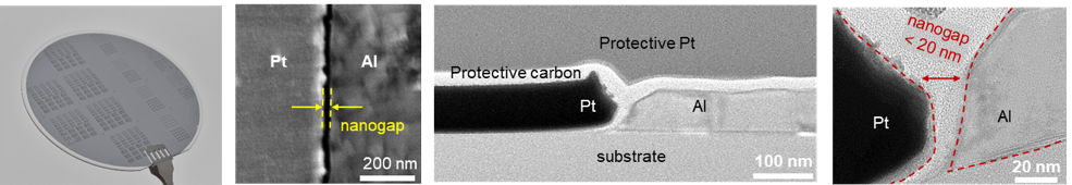
“There is more than Moore” to circumvent the plateau of Moore’s law, the electronics community drives an alternative, simple & scalable large area fabrication routes. Here at KAUST our group working on the development of sub-20 nm co-planar symmetric/asymmetric nanogap electrodes fabricated on glass/arbitrary substrates using a technique so called adhesion lithography (a-lith) by combining the conventional top down & the emerging bottom up self-assembly approaches. We further developing high performance functional devices such as diodes, photo-detectors (PDs), sensors, transistors and planar nano-LEDs to name but a few by incorporating suitable semiconductor/dielectrics atop of the nanogap electrodes. Using this rather simple nano-gap device architecture in combination with solution processing, we had demonstrated diodes with operating characteristics significantly higher than 100 GHz which paves the way to a radically new diode technology that has the potential to significantly powering the IoT devices. Our nanogap devices team further developing planar ICs such as logic circuits, PDs arrays & voltage multipliers monolithically on arbitrary substrates to validate our technology in many other possible applications & device incorporations.