16 June, 2020
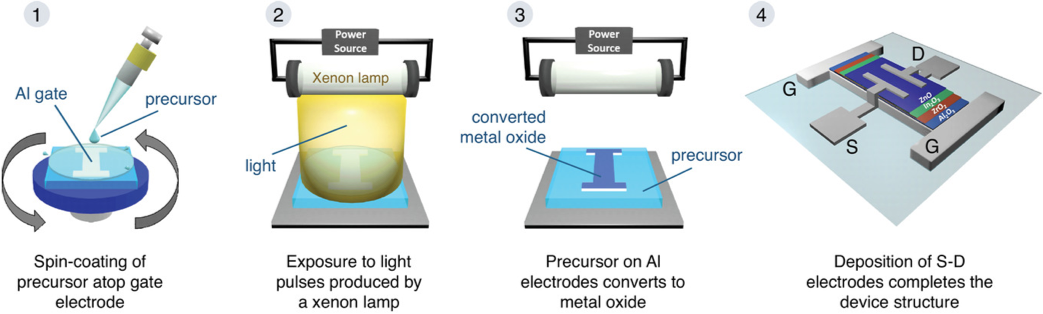
Congratulations Emre Yarali and co-authors for their recent paper on Advanced Electronic Materials titled "Low‐Voltage Heterojunction Metal Oxide Transistors via Rapid Photonic Processing". In this paper, a rapid photonic curing process for metal oxide hetero-structures (both semiconductors and dielectrics) for TFTs has been demonstrated.
Abstract
Solution‐processed metal oxide thin‐film transistors (TFTs) represent a promising technology for applications in existing but also emerging large‐area electronics. However, high process temperatures and lengthy annealing times represent two remaining technical challenges. Different approaches aiming to address these challenges have been proposed but progress remains modest. Here, the development of high electron mobility metal oxide TFTs based on photonically converted Al2O3/ZrO2 and In2O3/ZnO bilayers acting as the high‐k dielectric and electron‐transporting channel, respectively is described. Sequential solution‐phase deposition and photonic processing lead to low substrate temperature (<200 °C) while minimizing the overall process time to less than 60 s without compromising the quality of the formed layers. The bilayer Al2O3/ZrO2dielectric exhibits low leakage current density (10−6 A cm−2 at 1 MV cm−1), high geometric capacitance (≈120 nF cm−2) and breakdown electric field of ≈1 MV cm−1. Combining Al2O3/ZrO2 with a photonically converted In2O3/ZnO heterojunction channels, results in TFTs with high electron mobility (19 cm2 V−1 s−1), low operation voltage (≤2 V), high current on/off ratio (>106), and low subthreshold swing (108 mV dec−1), that can be manufactured even onto thermally sensitive polymer substrates. The work is a significant step toward all‐photonic processed metal oxide electronics.