06 July, 2020
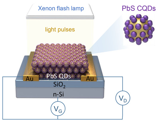
ABSTRACT: Recent advances in solution-processable semiconducting colloidal quantum dots (CQDs) have enabled their use in a range of (opto)electronic devices. In most of these studies, device fabrication relied almost exclusively on thermal annealing to remove organic residues and enhance inter-CQD electronic coupling. Despite its widespread use, however, thermal annealing is a lengthy process, while its effectiveness to eliminate organic residues remains limited. Here, we exploit the use of xenon flash lamp sintering to post-treat solution-deposited layers of lead sulfide (PbS) CQDs and their application in n-channel thin-film transistors (TFTs). The process is simple, fast, and highly scalable and allows for efficient removal of organic residues while preserving both quantum confinement and high channel current modulation. Bottom-gate, topcontact PbS CQD TFTs incorporating SiO2 as the gate dielectric exhibit a maximum electron mobility of 0.2 cm2 V−1 s −1 , a value higher than that of control transistors (≈10−2 cm2 V−1 s −1 ) processed via thermal annealing for 30 min at 120 °C. Replacing SiO2 with a polymeric dielectric improves the transistor’s channel interface, leading to a significant increase in electron mobility to 3.7 cm2 V−1 s −1 . The present work highlights the potential of flash lamp annealing as a promising method for the rapid manufacture of PbS CQD-based (opto)electronic devices and circuits. KEYWORDS: colloidal quantum dots, thin-film transistors, flash lamp annealing, solution-processed semiconductors, large-area electronics